15th April 2019, updated at 11pm on the 15th April
I've managed to get the 74LS593 chips to work in a circuit. This might be a long post, so I'll start with links to the datasheets again:
You might also want to read my initial notes on the 74LS593 which identifies some discrepancies in the datasheets.
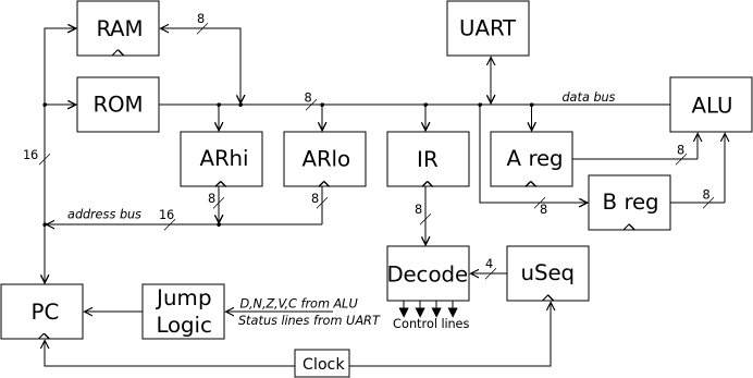
I want to use two 74LS593s in a TTL CPU that I'm designing which has this top-level structure:
I want the PC (two 74LS593 chips) and the address register (AR, two 74HCT574 chips) to be connected to a shared address bus. Both types of chips are tri-state, so they can take turns asserting a value on the bus.
I need the PC to be able to:
Here is the waveform diagram given in the Texas Instruments datasheet:
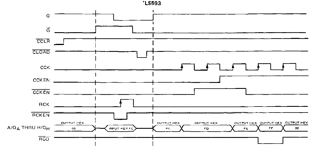
With G high and G# low, the 593 asserts a value on the output. G goes low, and so does RCKEN#, to accept an input. When RCK strobes high, the value is loaded into the 593 register. Then, CLOAD# goes low to transfer the register value into the counter.
At this point, G can be raised to assert the counter's output again. From this point on, with CCKEN and CCKEN# set correctly, a strobing CCK will increment the counter's value.
From this, it seems that we can tie G and RCKEN# together and drop them at the same time to load the input into the 593 register. While not explicitly shown, I wondered if I could raise RCK and lower CLOAD# at the same time to move the input into the 593 register and immediately into the 593 counter.
I've also learned my lesson and I won't use the system clock for RCK or CCK. This is because the ROM outputs are substantially delayed (e.g. 70nS) compared to the system clock. So, if I try to increment the counter value by setting CCKEN or CCKEN# from the ROM, the system clock will arrive at the 74LS593 first and the counter won't get incremented.
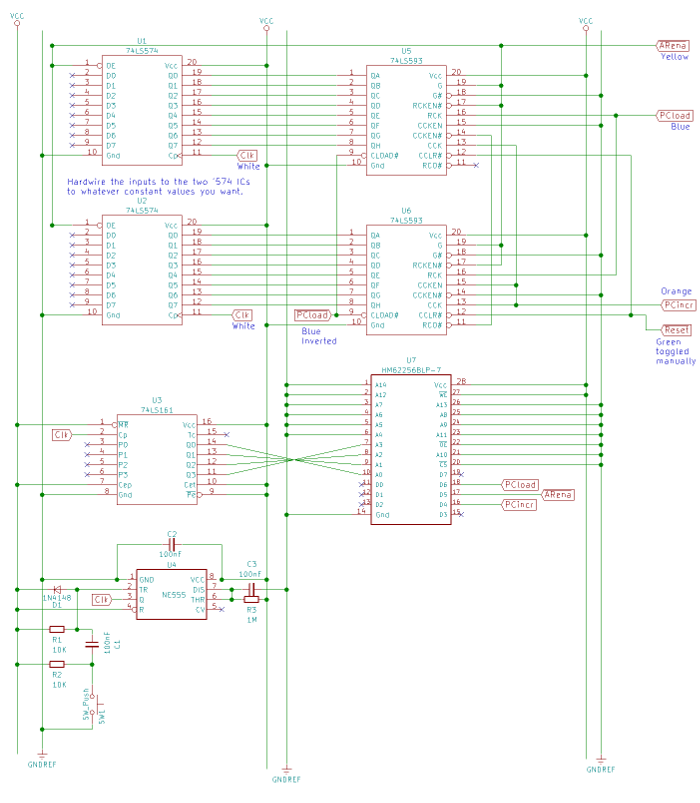
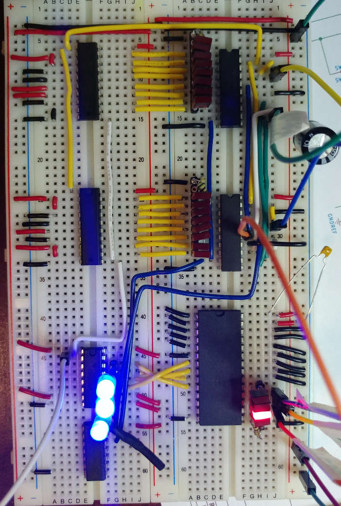
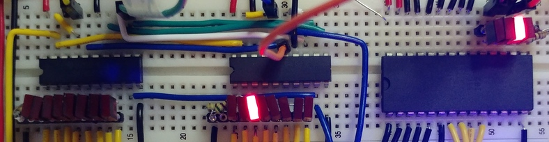
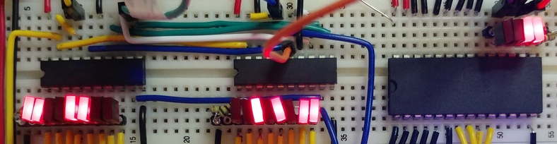
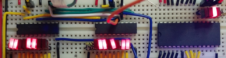
So here is my new test circuit. On the top-left are the two 74HCT574 address register chips, and on the top-right are the two 74LS593 PC chips. Below these are a 74HCT161 counter (middle-left) which provides an increasing sequence of sixteen values to the ROM (middle-right), so I can generate a sequence of sixteen control operations on the AR and PC.
I've wired the 74LS593 G, RCKEN# and the 74HCT574 OE# lines together as the ARena# control line. When low, AR asserts the value on the address bus and the PC is primed to load it. When high, the PC asserts the value on the address bus.
The next control line is the PCload line: this is tied to RCK and its inverse is tied to CLOAD#. When low, nothing happens. When ARena# is low and PCload goes high, this triggers the load into the 74LS593 register and hopefully also into the 74LS593 counter.
The third line is PCincr, tied to the low 74LS593 CCK and CCKEN, with CCKEN# tied low. When PCincr goes high and we are not loading a value into the 74LS593, the 74LS593 counter will increment.
On the high 74LS593, CCKEN# gets the active low carry from the RCO# output from the low 74LS593, CCKEN is tied high, and CCK is also connected to PCincr.
All three of ARena#, PCload and PCincr are generated from a ROM. In the final CPU, this will be the ROM holding the microcode. The fourth line, Reset, is triggered manually to reset the CPU. Here, I'll simply move the wire connected to the 74LS593 CCLR# line to reset the PC value.
Here is the breadboard version. The 555 is out of shot, and the bottom-left chip (under the lowest blue LED) is a 74HCT04 hex inverter used to invert the PCload line to make the CLOAD# line.
I've wired PCload to ROM D6, ARena# to ROM D5 and PCincr to ROM D4. Thus, we should have these useful ROM byte values:
| PCload | ARena# | PCincr | Byte Value | Action |
|---|---|---|---|---|
| 0 | 0 | 0 | 0x00 | Assert AR on the bus |
| 0 | 1 | 0 | 0x20 | Assert PC on the bus |
| 0 | 1 | 1 | 0x30 | Increment and assert PC on the bus |
| 1 | 0 | 0 | 0x40 | Load from the AR value on the bus |
I have set up the first sixteen ROM locations to have these values and hence this sequence of actions:
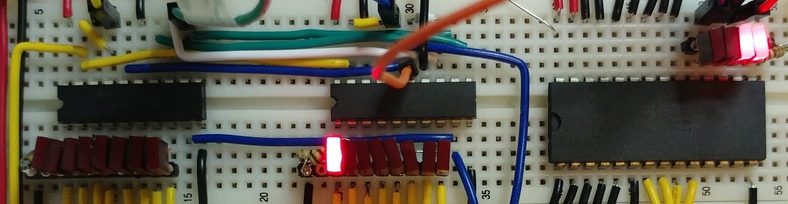
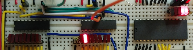
The following are photos of the test; each one is followed by a description. Each photo shows the ROM value and the address bus value after I have strobed the clock signal.
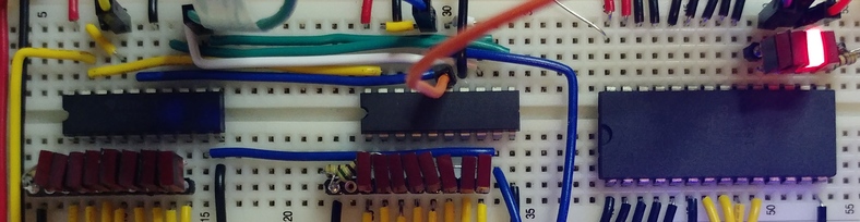
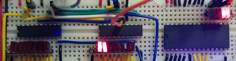
The above image shows the high PC chip on the left with eight LEDs. Due to the wiring, the PC value is backwards (lsb on the left). In the middle is the low PC chip, again with eight LEDs (lsb on the left). On the right is the ROM with four LEDs showing the value 0010 (2). This is the final ROM sequence value. I've just manually reset the PC value.
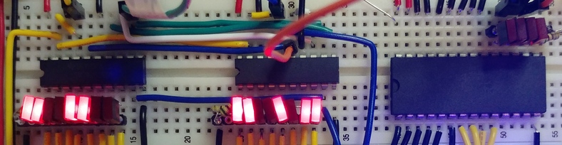
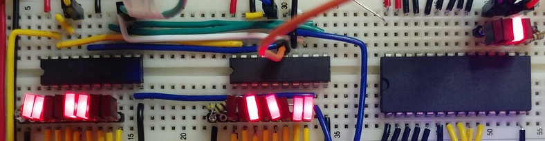
Sequence 0: above, we have clocked to the next ROM value, 3, which increments the PC.
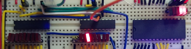
Sequence 1: above, we have clocked to the next ROM value, 3, which increments the PC again: now at value 2.
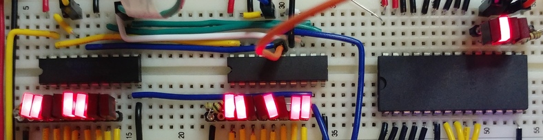
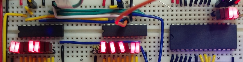
Sequence 2: ditto: now at value 3.
Sequence 3: ditto: now at value 4.
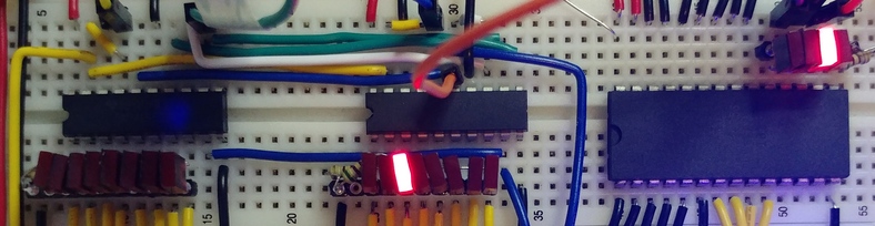
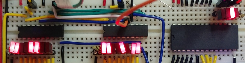
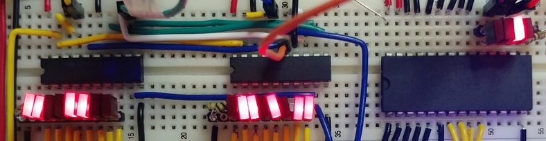
Sequence 4: above, the ROM is now value 2 which shows the PC value.
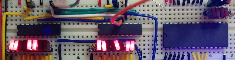
Sequence 5: Above, the AR is asserted on the address bus. This happens immediately as ARena# doesn't need to be clocked. The AR value is 0011 0011, 1101 0011 which I have hardwired on the breadboard.
Sequence 6: Above, the ROM value is 2, again asserting the PC value of 4 on the bus.
Sequence 7: Above, the ROM value is 0, placing the AR on the bus again.
Sequence 8: Now it gets interesting. Above, the ROM value is 4. The PC is being loaded from the AR whose value is asserted on the bus.
Sequence 9: Above, the ROM value is 2, asserting the PC value on the bus. You can see that the PC value is now the AR value 0011 0011, 1101 0011.
Sequence 10: Above, the ROM value is 3 which increments the PC to the value 0011 0011, 1101 0100.
Sequence 11: Above, the ROM value is 2, asserting the PC value on the bus.
Sequence 12: Above, the ROM value is 3 which increments the PC to the value 0011 0011, 1101 0101.

Sequence 13: Above, another increment. The PC is now 0011 0011, 1101 0110.
Sequence 14: Above, show the PC value which is still 0011 0011, 1101 0110.
Sequence 15: Above, show the PC value as before.
Finally, I have got the 74LS593 to do what I want: share the address bus, load a value from the address bus and increment its value.
However, it took me three iterations through my test circuit (and nearly giving up) to get it here. I hope, if you are thinking of using the 74LS593 chips yourself, that you found this useful.
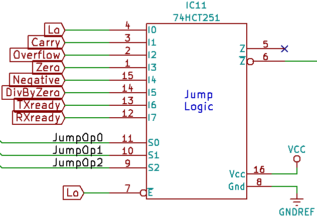
One last note. In my CPU design which will use the 74LS593, the PCload line will be generated by a 74HCT251 8:1 multiplexer. This has both inverted and non-inverted outputs, so luckily I won't need yet another inverter to drive CLOAD#. I haven't updated my schematic yet.
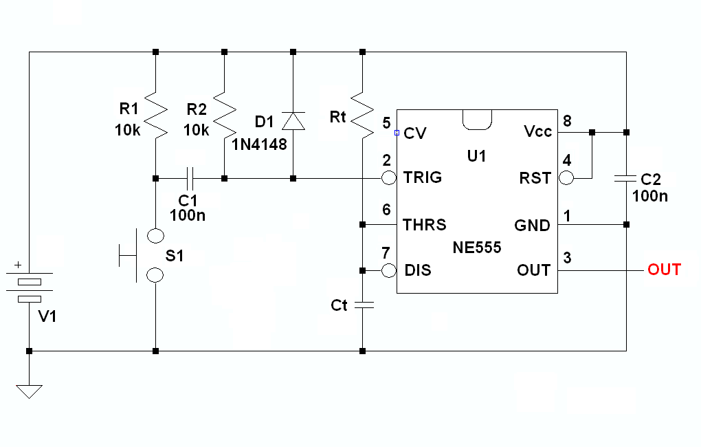
For the above test circuit, I got the key debounce circuit from this stackexchange post by EM Fields.