Answers to 2010 January Semester
Mid-term Examination
INFT13-600 and 73-600
Special Topic in IT
Question 1 - Multiple Choice
The correct answer is shown in bold font.
- Every boolean expression of N inputs and one output can be implemented
- using a combination of D flip-flops, multiplexors and registers.
- by connecting the output directly to all of the N inputs.
- using a combination of And and Or gates.
- using a combination of And, Or and Nand gates.
Comment: We know that we need And, Or and Not, but we also
know that Nand can create And, Or and Not, so d) is the right answer.
- In twos-complement arithmetic, to create a negative value of a number
X:
- invert (Not) every bit in the number X.
- invert the most significant bit of X.
- add 1 to X, and invert every bit.
- subtract 1 from X, and invert every bit.
Comment: the usual rule to create a negative value is to
invert every bit then add 1. So to create -X from +X, invert and add
1. But this also means that we can create +X from -X by inverting
-X and adding 1. Therefore, working backwards, we can create -X from
+X by subtracting 1 from +X, and then inverting the bits.
- In the HDL implementation of the Bit chip, the output from the DFF
is connected to the input of the Mux. This is done
- to convert the Mux into a sequential chip.
- to ensure that the Bit value is retained after each clock
cycle if load is off.
- to ensure that the new input bit is stored on every clock cycle.
- to ensure that the Bit value is retained after each clock cycle if
load is on.
Comment: the Bit's value is recycled only when load is off.
Otherwise, the input is multiplexed into the DFF.
- The A-instruction in the Hack computer performs
- direct addressing.
- immediate addressing.
- indirect addressing.
- bitwise addressing.
Comment: There is no such thing as d) bitwise addressing.
Direct addressing is where, given an address, the value of memory
at that location is loaded. Indirect addressing is where a memory
location's value is used as a pointer or reference to
another memory location, whose value is loaded. The A-instruction
does not access any data memory locations, so a) and c) are out. The
A-instruction loads a constant into the A-register: this is b) immediate
addressing.
- Each memory address in the Hack computer references
- a single byte.
- a single word.
- multiple words.
- the D-register.
Comment: When the Hack CPU loads data from data memory, it
places an address on the Memory address bus, and receives back a 16-bit
value. Thus, it is not a byte, nor is it multiple words. The 16-bit
value is a single word.
Question 2
The C-instruction in the Hack computer has the following structure:
1 1 1 a c1 c2 c3 c4 c5 c6 d1 d2 d3 j1 j2 j3
where the a bit selects either the A-register or memory, the
six c bits define what instruction is to be performed, the
three d bits define the destination of the instruction result,
and the three j bits define what jump operation (if any) should
be performed.
Most computer architectures have the concept of a no-operation instruction,
NOP, which has no effect on the state of the CPU except increment
the program counter to address the next instruction. Find and write
down a Hack C-instruction (i.e a specific pattern of 16 bits) which
is equivalent to a NOP, i.e. which has no effect on the CPU except
increment the program counter.
In your answer, explain why the instruction that you specified has
no effect on the CPU state.
Answer to Question 2
We need an instruction which does not store the ALU's result anywhere,
nor does it cause the CPU to jump to a different instruction than
the next one. Looking at the C-instruction's format, we need to set
d1 d2 d3 to 0 0 0, and j1 j2 j3 also to 0 0 0. It
does not matter what the ALU is instructed to do, as its result will
never be used. Therefore, there are a whole set of NOP C-instructions:
1 1 1 X X X X X X X 0 0 0 0 0 0
where X stands for any single-bit value. There is no destination for
the ALU result, so the CPU's state is not modified. The j1
j2 j3 == 0 0 0 bits ensure that no jump is performed, so the PC will
increment and load the next instruction.
Question 3
Estimate the number of NAND gates in:
- a half-adder
- a 16-bit full-adder
Show the working that you used to arrive at your estimates.
Answer to Question 3
My half-adder design uses an And gate and an Xor gate. My And design
uses two Nand gates, and my Xor design uses four Nand gates. Thus,
a 1-bit half-adder can be made from 6 Nand gates.
Each 1-bit full-adder that I designed is made from:
- two Xor gates, i.e. 8 Nand gates
- two And gates, i.e. 4 Nand gates
- one Or gate, using 3 Nand gates from my Or design
Thus, each 1-bit full-adder requires 15 Nand gates. A 16-bit full-adder
can be made from 16*15 or 240 Nand gates.
Question 4
The following diagram shows a logic circuit using a combinatorial
chip called A, and a sequential chip called B.
Explain why the wiring around chip B is legal, but the wiring around
chip A is not legal.
Answer to Question 4
Chip B is sequential, so the output from B at time t depends
on the a and b inputs from time t-1. Chip A,
on the other hand, is combinatorial: the output occurs instantaneously
given the a and b inputs. As A's output is connected
to the a input, this creates a feedback loop, which means that
the output from A is completely unpredictable. The classic example
is that of a Not chip whose output is connected to its input: what
is the value of the output? It cannot be true, as true is also the
input; ditto for false.
Question 5
The following gives the HDL interface definition of a chip called
High4:
    CHIP High4 {
      IN in[4];
      OUT out[2];
    }
The purpose of the chip is to output a 2-bit integer that represents
the number of the highest input bit which is on. For example, if in[2]
is the highest input bit on, the output is 1,0; similarly, if in[1]
is the highest input bit on, the output is 0,1. The full truth table
for the chip is given below.
| in[3] | in[2] | in[1] | in[0] | out[1] | out[0] |
|
| 0 | 0 | 0 | 0 | 0 | 0 |
| 0 | 0 | 0 | 1 | 0 | 0 |
| 0 | 0 | 1 | 0 | 0 | 1 |
| 0 | 0 | 1 | 1 | 0 | 1 |
| 0 | 1 | 0 | 0 | 1 | 0 |
| 0 | 1 | 0 | 1 | 1 | 0 |
| 0 | 1 | 1 | 0 | 1 | 0 |
| 0 | 1 | 1 | 1 | 1 | 0 |
| 1 | 0 | 0 | 0 | 1 | 1 |
| 1 | 0 | 0 | 1 | 1 | 1 |
| 1 | 0 | 1 | 0 | 1 | 1 |
| 1 | 0 | 1 | 1 | 1 | 1 |
| 1 | 1 | 0 | 0 | 1 | 1 |
| 1 | 1 | 0 | 1 | 1 | 1 |
| 1 | 1 | 1 | 0 | 1 | 1 |
| 1 | 1 | 1 | 1 | 1 | 1 |
Design a HDL implementation (or a logic circuit diagram) of the High4
chip which correctly implements the truth table. Also provide a short
description of how your design implements the required functionality.
Answer to Question 5
There are, of course, several ways to answer this. You could treat
the outputs as two independent functions, and apply boolean algebra
using Ands, Ors and Nots to produce the correct results. You can also
look for patterns in the truth table to minimise the number of gates
used. Here is my answer.
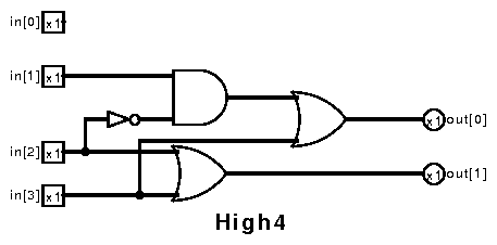 Looking at the table, the in[0] input has no effect on the output:
when the other bits are constant, changing in[0] has no effect.
The value of out[1] is only true when either in[2] or in[3]
is true, so an Or gate can be used to produce the out[1] value.
For out[0], it seems that either in[3] has to be true, or
otherwise in[2] is false and in[1] is true. Thus, in the diagram,
in[2] is negated and Anded with in[1]. This is then Or'd with
in[3] to get the final output.
Looking at the table, the in[0] input has no effect on the output:
when the other bits are constant, changing in[0] has no effect.
The value of out[1] is only true when either in[2] or in[3]
is true, so an Or gate can be used to produce the out[1] value.
For out[0], it seems that either in[3] has to be true, or
otherwise in[2] is false and in[1] is true. Thus, in the diagram,
in[2] is negated and Anded with in[1]. This is then Or'd with
in[3] to get the final output.
File translated from
TEX
by
TTH,
version 3.80.
On 25 Feb 2010, 20:35.