I wanted to implement my microcoded CPU on real hardware, as it were, so I first converted it to VHDL using GHDL as the platform. Then I bought a Nexys4 DDR development board to run the CPU on real silicon. The CPU design is essentially the same as the original, but with changes (as per the GHDL version) to give it ROM, RAM and a UART. I also use the LEDs and switches on the Nexys4 board to control the CPU and to give diagnostic output.
Here is a Zip file which contains the microcoded CPU in VHDL format ready to run on a Nexys4 DDR board. It should run on the previous Nexys4 board and on other FPGA development boards with a few changes to the top-level VHDL file.
Most files are copyright Warren Toomey and are distributed under the GPL3 licence; some were written by other people. I would recommend that you read through the details of the CPU and the assemblers before bringing the CPU up on an FPGA platform.
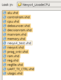
Unpack the Zip file. You should see these files:
Nexys4DDR_Master.xdc
UART_TX_CTRL.vhd
alu.vhd
controlrom.vhd
cpu.vhd
debouncer.vhd
decisionrom.vhd
mainrom.vhd
memory.vhd
nexys4.bit
nexys4.vhd
nexys4_test.vhd
prog_cntr.vhd
ram.vhd
reg.vhd
regfile.vhd
ulogic.vhd
Start up Vivado and create a new project called Nexys4_UcodeCPU. Create an RTL project. Add all of the .vhd files (except nexys4_test.vhd) as the source files to the project.
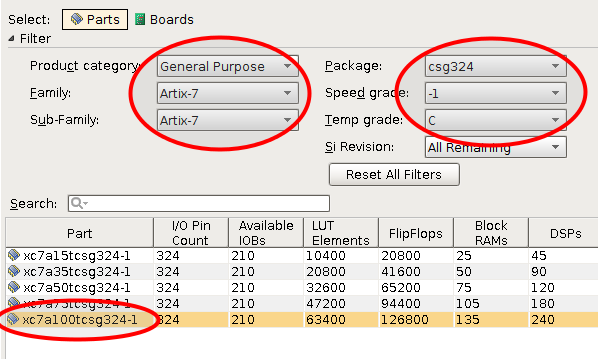
Copy the source files into the project, and mark the language as VHDL. Skip the Existing IP window. Add Nexys4DDR_Master.xdc as the constraint file. Choose the xc7a100tcsg324-1 part by using the filter choice shown in the following image:
You should now see the main project window. Over on the left, choose Add Sources and add nexys4_test.vhd as a simulation source. Under Project Settings → Simulation Settings, choose nexys4_test as the simulation top module name. Under Project Settings → General Settings, ensure that nexys4 is the top module name.
The project is ready to build. You can now run a behavioural simulation, run synthesis, run implementation and generate a bitstream.
To do this you need a working bitstream file for the Nexys4 board. Create this using the project in Vivado, as above, or use the nexys4.bit file that came in the original Zip file. Copy this to your Nexys4 board and turn on the board. Make sure that you have the micro USB port connected to a computer which is running a terminal program and listening to the Nexys4's UART. On Linux, I use minicom -b 9600 -D /dev/ttyUSB1, and I make sure that my user belongs to group dialout so I have permission to use /dev/ttyUSB1.
If you have your terminal program set up correctly, you will see the CPU run a program that displays this output:
Here are two numbers followed by their sum:
3142
23
3165
After that, the program will prompt you to type some characters on the terminal; these will be echoed back to you.
You will also see the 7-segment LEDs, the tricolour LEDs and the row of green LEDs show something, but as the CPU is running at 500 kHz this will be a blur. Here is what the LEDs are displaying:
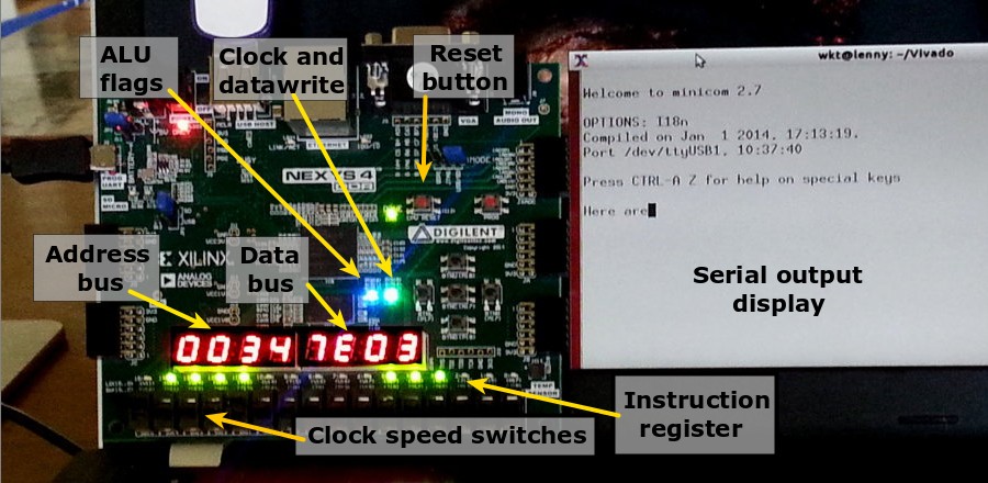
The left four 7-segment LEDs display the value on the address bus. The right four 7-segment LEDs display the value on the data bus. Underneath these, the row of green LEDs show the value stored in the Instruction Register in binary.
The rightmost tricolour LEDs shows the system clock cycling in green, and red when the datawrite line is enabled, i.e. when something is being written to memory. The leftmost tricolour LED shows the ALU flags: carry is red, zero is green, negative is blue. The image above shows the address bus with value 0x0034, data bus 0x7E03, the clock in the high part of the cycle and the ALU producing a negative output.
The speed of the CPU can be controlled by the six leftmost slide switches: SW15 down to SW10. If SW15 (leftmost) is raised, the clock is stopped. You can then single-step the CPU by pressing the right-most pushbutton. Remember that each machine instruction takes several clock cycles, so you need to press it multiple times to see anything happening.
If you just want to slow the CPU down but keep it running, raise only one of SW14 … SW10 and lower SW15. These switches give you a clock rate of 1Hz (SW14), 2Hz, 4Hz, 10Hz and 20Hz (SW10), respectively.
If you want to reset the CPU and restart the program built into the ROM, hold down the red CPU reset button and release it.
There is no simple way to do this because the ROM contents are in the bitstream file; you have to change the contents of the mainrom.vhd source file and generate a new bitstream. If you do want to do this, I would recommend that you download the GHDL version of the CPU, modify the basic_program.s assembly language file, and run make main.rom. This should run the two commands:
./massem basic_program.s 2> /dev/null
./gen_rom main.rom 14 16 mainrom.vhd
Now copy the mainrom.vhd file into the Vivado project (replacing the existing file) and rebuild the bitstream for the CPU.
The Nexys4 version of the microcoded CPU is derived from the GHDL version of the CPU. The main difference against the Logisim version is that this version has 16K of ROM, 16K of RAM and a memory-mapped UART for serial I/O. You may want to read the details on the GHDL version web page.
The Nexys4 version of the CPU differs from the GHDL version as well:
The top level component is now the nexys4.vhd file which captures the board-specific code, and makes the code in cpu.vhd and memory.vhd more generic. This will allow this code to be more easily ported to other FPGA boards.
The GHDL version used tri-state logic to control the data bus. I could not work out how to do this on a real FPGA. Based on the advice I received on several forums, I rewrote the code to ensure that the data bus has a single driver.
The GHDL version allows the contents of the three ROMs (the main ROM and the microcode decision & control ROMs) to be loaded directly from files. The Nexys4 version has to have everything contained in the bitstream, so now there are three xxxrom.vhd files which have their contents hard-coded. They are generated from the xxx.rom files which are in the GHDL version of the CPU.
For my reflections on the process of doing this, see the bottom of the original CPU web page.
Warren Toomey, July 2015