Introduction
I asked myself:
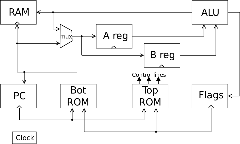
"Crazy idea: what's the smallest number of 7400-style chips
needed to build a CPU?". This is the result, my "crazy
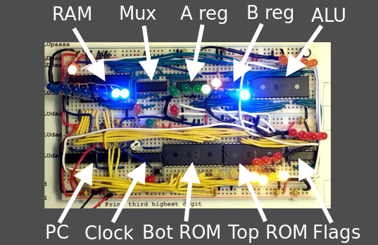
small" CPU. I've implemented it both in Logisim and also with
real chips on two breadboards. The chip count ended up as
three ROMs, one RAM, three registers, two counters, one multiplexer
and one timer for a total of eleven chips.
The CPU has a 4-bit
data path with an 8-bit address space (256 4-bit words). There are
two 4-bit data registers, A and B, which can be loaded across the
data bus from the RAM. The A and B values are sent to the ALU, which
can perform sixteen different operations. The ALU result can be placed
back on the data bus for writing back to RAM.
Using the
multiplexer, both the A and B registers can be loaded either from RAM or from
part of the current instruction. This allows constant literal
values to be used in the program.
The instruction
sequence is controlled by the 8-bit Program Counter (PC) which
normally increments. The PC's value chooses a location in the top and
bottom ROMs. The bottom ROM's value is the RAM location to access on
this instruction. The top ROM's value encodes the six control signals
for the CPU:
ALUop (3 bits): which ALU operation to perform
PCincr (1 bit): increment the PC (high) or load the PC (low)
Aload (1 bit, active low): load the A register from the multiplexer (low)
Bload (1 bit, active low): load the B register from the multiplexer (low)
Asel (1 bit): when loading a register, get data from the instruction (low) or from RAM (high). This control line
serves a dual purpose. It also acts as an ALUop bit, giving the ALU sixteen operations.
RAMwrite (1 bit, active low): when high, read from RAM onto the data bus;
when low, read from the ALU onto the data bus and write it to RAM
Finally, the ALU
outputs four result flags: negative (N), zero (Z), overflow (V) and
carry (C). These are buffered in the Flags register at the end of each
instruction to be used on future instructions.
The CPU can perform
jumps. When the PCincr control line is low, the address from the
bottom ROM is loaded into the PC, "jumping" to a new
instruction. To do conditional jumps, the two ROMs receive and
combine the PC's value and the NZVC value as the ROM address
to look at. This means that there are sixteen ROM "pages",
one for each combination of NZVC flags.
So here is where it
gets tricky. If you want the CPU to keep running one instruction
after the other, you need to write the instruction sequence in all 16
pages on the ROMs. Thus, regardless of what the NZVC flags are, the
correct next instruction will be found.
So, how is a
conditional jump like JCS (jump to location X if carry is set) done?
Assume that this instruction occurs at location 12 in the instruction
sequence. At location 12 on the eight ROM pages which would be
accessed when the C flag is set, a "jump" instruction is
encoded. At location 12 on the other eight ROM pages, a "nop"
instruction is encoded. Only when the C flag is set will the ROMs
access the pages with the "jump" instruction and jump.
Otherwise, the CPU will perform the "nop" instruction and
move onto the next instruction.
The ALU Operations
The ALU can perform
sixteen operations based on the A and B inputs:
A + B decimal
A - B decimal
A & B
A | B
A ^ B
A + 1
Output 0, flags set to B's value
Output 0
A + B binary
A - B binary
Output A
Output B
A * B binary, high nibble
A * B binary, low nibble
A / B binary
A % B binary
The negative (N), zero (Z), overflow (V) and carry (C) flags
are set after each ALU operation except the decimal operations.
The "Output A"
and "Output B" operations allow the ALU to pass the A and B
registers through so they can be written out to RAM.
The ALU is
implemented as a 8K x 8 bit ROM. As input it takes four A bits, four
B bits, a carry in bit and the four ALUop bits (including Asel). The output is the four
result bits and the four flag bits. The ROM simply looks up the result based
on the input.
The binary and decimal addition and subtraction operations take and use
the carry in bit. This allows N-bit or N-digit additions and subtractions.
Instruction Format
Taking the top and
bottom ROMs as a single 16-bit wide ROM, here is the instruction
format.
|
RAMwrite (active low)
|
Asel
|
Bload (active low)
|
Aload (active low)
|
PCincr
|
ALUop
|
RAM/ROM address
|
|
X
|
X
|
X
|
X
|
X
|
XXX
|
AAAAAAAA
|
This means that the
CPU is already hard-wired to perform certain instructions: we just
need to determine which instructions are actually useful. For example:
|
Load A with constant from ROM
|
LCA AAAA
|
10101 xxx xxxxAAAA
|
|
Load A from memory
|
LMA AAAAAAAA
|
11101 xxx AAAAAAAA
|
|
Load B from memory
|
LMB AAAAAAAA
|
11011 xxx AAAAAAAA
|
|
Store A to memory
|
SMA AAAAAAAA
|
00111 101 AAAAAAAA
|
|
Store B to memory
|
SMB AAAAAAAA
|
00111 110 AAAAAAAA
|
|
Put A+B to memory
|
ADDM AAAAAAAA
|
00111 000 AAAAAAAA
|
|
Put A-B to memory
|
SUBM AAAAAAAA
|
00111 001 AAAAAAAA
|
|
Jump to ROM address
|
JMP AAAAAAAA
|
10110 xxx AAAAAAAA
|
|
No operation
|
NOP
|
1x111 xxx xxxxxxxx
|
Example Program
Here is an example
program which calculates the first Fibonacci numbers which fit into
four bits. The columns shown are: instruction number, instruction, operand,
hex encoded instruction, list of active control lines, comment.
00: LCA 1	a801	Aload 		   # Store 1 in locations 0 and 1
01: SMA 0	3d00	RAMwrite ALUpassa
02: SMA 1	3d01	RAMwrite ALUpassa
03: LMA 0	e800	Asel Aload 	   # Load RAM location 0 into A
04: LMB 1	d801	Asel Bload 	   # Load RAM location 1 into B
05: ADDM 2	3802	RAMwrite ALUadd    # Add them and store in location 2
06: JCS end	b00c	                   # Result too big, exit the loop
07: LMA 1	e801	Asel Aload 	   # Copy RAM location 1 down to 0
08: SMA 0	3d00	RAMwrite ALUpassa
09: LMA 2	e802	Asel Aload 	   # Copy RAM location 2 down to 1
0a: SMA 1	3d01	RAMwrite ALUpassa
0b: JMP loop	b003	                   # Go to instruction 3 to do it again
0c: JMP end	b00c			   # End: do an infinite loop
If you run
this in the Logisim version, you can see the last three values of the
Fibonacci sequence in the first three RAM locations.
A ROM for an ALU?
Is implementing the
ALU with a ROM fair game, or is it breaking the rules? You could
argue either way. I could have hunted down a 74LS181 ALU to make the
design really authentic. I'd need two more control lines for the five
select/mode bits. Anyway, it's still one chip for the ALU, so the
choice doesn't have
too much of an impact on the design. A ROM also allows the designer
to choose what ALU operations can be performed.
Design Changes
The chip count can be reduced. Right now I'm using two 74LS161 chips for
the PC, but there is an obsolete 74LS469 chip that could replace both of
them. That would bring the chip count down to ten. Next up, replace the
two control ROMs with an AT27C1024 64Kx16 ROM chip (the only x16 ROM I could
find): that would bring the chip count down to nine. Finally, the A and B
registers could be replaced with one CD4508B dual 4-bit register as it
has separate load lines: that would bring the chip count down to eight chips.
I'll probably never do this as I would have to rewire the whole thing!
There is only one carry bit input and output by the ALU; this really limits any
shift left/right operations to one bit shifts.