I just got a good comment from John Lonergan on one of my Youtube video about my 4-bit CPU, the CSCv2:
Could you please put something together specifically addressing the question of synchronising changes to the control lines with the clocking of the sequential components.
Given that I spent a heap of time ironing out timing issues with my new 8-bit CSCvon8 CPU, I thought I'd answer John's question by looking at the CSCvon8 architecture and how the clock signal propagates in it.
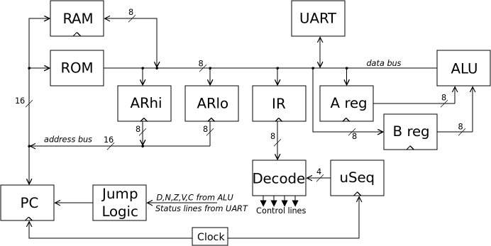
Above is the essential architecture for the CSCvon8. It's a von Neumann architecture where the data and instructions are brought into the CPU from RAM/ROM across the data bus. There are two data registers, A and B; these provide the input to the ALU.
For conditional jump instructions, the location to jump to is loaded into the address registers ARhi and ARlo. The ALU calculates a value and also some flags (e.g. zero, negative). The Jump Logic decides if the Program Counter (PC) should jump or not, and it tells the PC to either increment to the next instruction location, or jump to a new instruction location.
The design is microcoded: the instruction byte is loaded into the instruction register (IR) on the zeroth phase of the sequence of microinstructions. This instruction value, along with the microsequence counter (uSeq) value looks up a location in the Decode ROM.
The Decode ROM stores 16-bit values. Each 16-bit value in the Decode ROM is the microinstruction to perform for that microsequence phase. A high-level instruction is composed of a sequence of microinstructions. As an example, here is the microsequence to load an 8-bit constant value from memory into the A register:
# LCA: Load A with constant $XX
    MEMresult IRload PCincr
    MEMresult Aload  PCincr
    uSreset
The zeroeth microinstruction tells the RAM to place the value that the PC points to on the data bus (MEMresult), the IR register to load this value (IRload) and the PC to increment (PCincr).
The next microinstruction tells the RAM to do the same thing. As the PC was incremented, it now points at the byte after the LCA instruction. This is loaded into the A register (Aload) and the PC incremented again. The PC now points at the next instruction byte.
The final microinstruction tells the microsequence counter (uSeq) to reset its value to zero (uSreset), so that it can fetch the next instruction byte into the IR register.
With the architecture out of the way, let's now look at the actual components. Now we move from the logical design to the actual physical implementation. For this discussion, the most important issue is the propagation delay through all the components. Here is a list of the components, what chip is used for it and the typical propagation delay for each chip.
| Component(s) | Chip | Propagation Delay |
|---|---|---|
| Databus reader demux | 74HCT138 | 21nS |
| Databus writer demux | 74HCT139 | 25nS |
| Microsequencer | 74HCT161 | 22nS |
| Jump logic | 74HCT151 | 20nS |
| Several registers | 74HCT574 | 30nS |
| Program counter | 74LS593 | 30nS |
| RAM memory | AS6C62256 | 55nS |
| ALU ROM | M27C322 | 45nS |
| Decode ROM | AT27C1024 | 45nS |
| Instruction ROM | 28C256 | 150nS |
Let's go back to the microsequence that loads the LCA instruction into the IR, and look at the propagation delays and how they affect the overall timing of the system.
Can you see the problem? The IR is ready to load the next instruction from ROM at 88ns, but the ROM won't place this value on the data bus until 242nS.
Somehow, we need to stall the loading of the IR until there is a valid value on the data bus.
We can solve this problem in several different ways. One way would be to have every component output both a new value and also a "data valid line". This would go low when the data output was invalid, and go high when the data is valid.
Each sequential component would have a "load data" line. When this line goes high, the component would load its new value from its inputs.
We would then connect the data output from one component to the data input of the next component. We would also connect the "data valid" line from the first component into the "load data" line of the next component. And this would result in an asynchronous design.
We don't have the option of an asynchronous design with the chips chosen for the CSCvon8. All the components simply change their output once it becomes ready, and there is no "data valid" line. Even worse, they all have different propagation values. So what is the solution here?
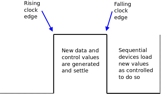
The solution is to see each clock pulse as having two halves:
Before we see how the above solution is implemented, we need to consider the issue of active high control lines and active low control lines.
From a logic standpoint, we like to think of the high logic value meaning something and the low logic value meaning nothing. Control lines which tell a device to do something when they are high are known as active high control lines.
Unfortunately, many of the TTL and CMOS logic chips are implemented where their control lines are active low. In other words, the chip will do something when the control line goes low.
Another thing we have to consider are chips which have their actions triggered by a particular logic level. As long as the level stays constant, they will continue to do the same action. Most combinational chips (e.g. AND gates, OR gates, multiplexers etc.) are level triggered. If their inputs change, their output changes. If their inputs stay the same, the output stays the same.
Most sequential devices are edge triggered. Their behaviour changes only when some control line's value changes. An example is a register which loads a new value from its inputs when its clock input rises. The clock signal is active high and the chip is edge triggered by the active high clock signal.
Go back and look at the high-level architecture design of the CSCvon8 again. We have several registers: A, B, ARhi, ARlo, PC and the uSeq counter. Some devices are combinational: the ROM and RAM output, the ALU and the Jump logic. Not shown are the various muxes and demuxes in the implementation of the CPU.
We need to generate new data and control values in the first half of the clock cycle. Once they are settled, we need to send the appropriate control lines to the sequential devices to load these data values, and we have to do this synchronously at the falling clock edge.
It turned out in the design that several chips are edge triggered by an active high (rising) signal, and others are edge triggered by an active low (falling) signal. Therefore, we have to generate an inverted clock signal; when clk rises, clkbar falls and vice versa. This is done with an inverter gate (from the schematic):
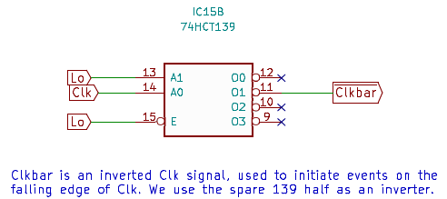
Unfortunately, I didn't have a spare inverter on my single 74HCT04 chip, so I had to use the spare half of my 74HCT139 to act as an inverter gate, as shown above.
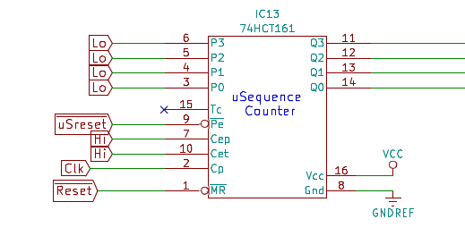
Let's now try to follow the clock signals throughout the design of the CSCvon8. Each new clock cycle starts with incrementing or resetting the 74HCT161 microsequence counter:
And that is literally the only place in the implementation where the rising clock signal gets used! What happens next?
The instruction in the IR, along with the microsequence phase number, goes to the Decode ROM to look up most of the control lines to output for this microinstruction:
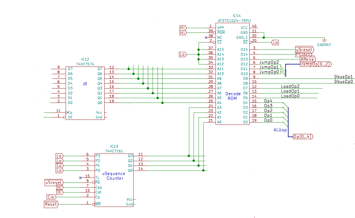
Remember, there is a 45nS delay through the Decode ROM. And there is no guarantee that all the output bits change at the same time, so we can't rely on the output bits to be synchronous, either.
It is complicated by the face that some of these control lines have to be split up further. The two DbusOp lines control three devices, and the three LoadOp lines control seven devices, and so we need some demultiplexers to do this:
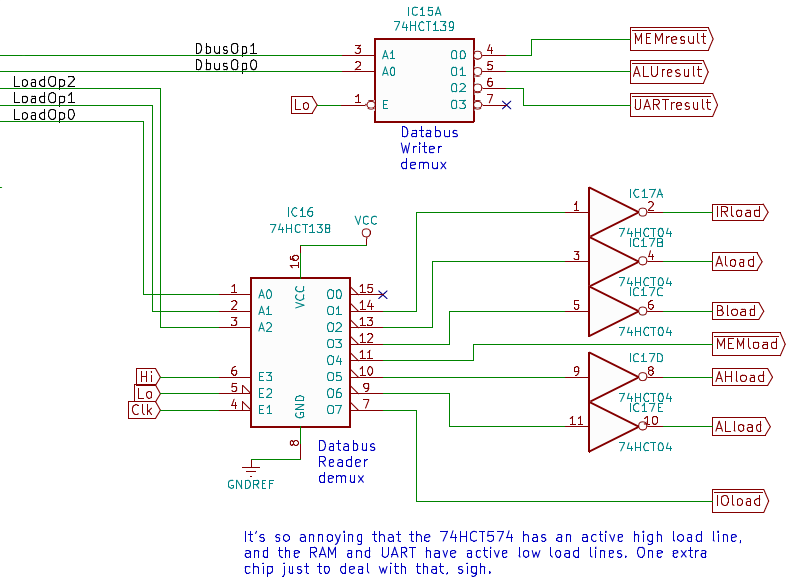
The MEMresult#, ALUresult# and UARTresult# control lines go directly to these three devices to tell which one can write on to the data bus in the first half of the clock cycle. There will be some propagation delays before the data bus has valid data on it. As long as the length of the first half of the clock cycle is long enough, we will meet the timing requirements.
We now need the seven XXload lines coming out of the 74HCT138 data bus reader demux to also settle during the first half of the clock cycle. Notice that some of these lines are inverted, but some are not.
Firstly, the 74HCT138 outputs active low values. This is fine for the RAM and ROM, as their write enable control inputs are active low (i.e. WE#); we can output MEMload# directly from the demux. Similarly, the IOload# line to the UART is active low.
But all the 74HCT574 registers have active high load lines. Therefore, we need to invert the control lines from the 74HCT138 before we wire them to the various registers; thus the five inverters shown in the above diagram.
But what I actually told you was a white lie. The 74HCT574 registers have active high edge triggered control lines. For each register to load appropriately, we need to raise its control line as required at the falling edge of the clock signal, i.e. at the beginning of the second half of the clock cycle.
How is this achieved? Luckily, the 74HCT138 demux has several enable control lines, E1, E2 and E3 (pins 4, 5 and 6). Here is the logic table for these lines from the data sheet:
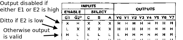
You should have noticed that E3 is wired high and E2 is wired low. E1 is wired to the clk signal. Therefore, all the load lines are inactive while the clock signal is high (i.e. in the first half of the clock cycle), but go active (with an edge) on the falling clock signal at the beginning of the second half of the clock cycle.
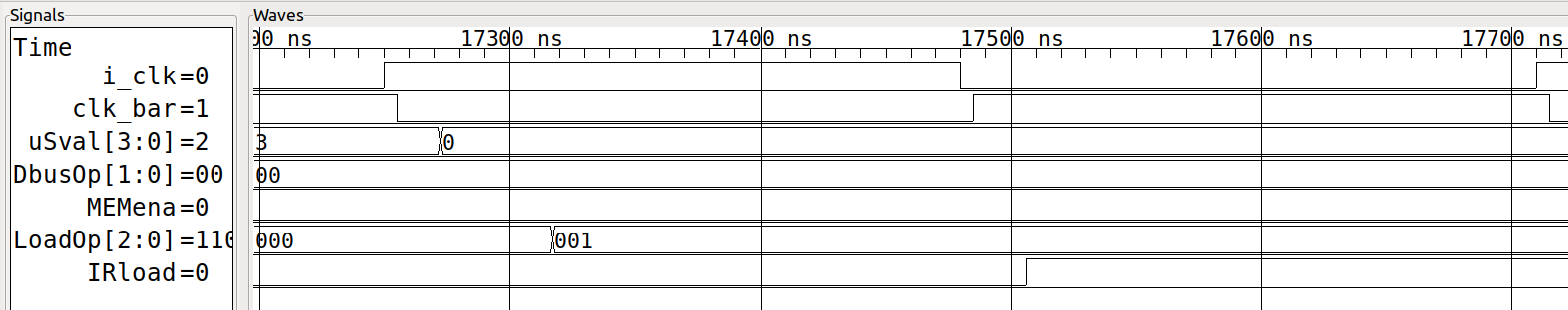
Above is a waveform of the loading of the instruction register (IR), which is the zeroeth microinstruction for all instructions on the CSCvon8. I generated this from my Verilog version of the CPU. This version models the propagation delays through the components, and it's a lot easier to generate the waveform here than to capture it from the real hardware!
Let's look at the waveform in detail. The top two waveforms are the clock signal, called i_clk here, and the inverted clock, clk_bar. Note that there is a delay in generating the clk_bar signal, as there is a propagation delay with the 74HCT139 that I'm using as an inverter.
When the clock signal changes on the microsequence counter, it also takes time to change its value (uSval), so there is a delay before it resets to value 0.
The uSval and the IR's value go into the Decode ROM; the new microinstruction value is output, and some of the output control lines go to the demuxes.
The MEMresult# line (called MEMena here) was 0 on the previous microinstruction and 0 here, so you can't see its value change at all.
On the other hand, the three LoadOp lines do change from binary 000 to binary 001. This happens only about a quarter of the way through the first half of the clock cycle. Even though they are settled, we must wait for the falling edge of the clock before we can demux them and send them to the appropriate data bus readers.
The clock signal, i_clk, falls in the middle of the captured waveform. You can see that, after a delay through the 74HCT138 demux, the IRload control line goes high. This goes to the IR and tells it to load the value which the memory device placed on the data bus in the first half of the clock cycle.
There is more of the story to be told here. But, rather than I explain it to you, I'll let you look at the CSCvon8 schematic and get you to work it out yourself.
Things to watch out for: