26th April 2019, updated 9th June 2019
After several days of breadboard experiments, I think I finally grok the 74LS593. Here's a summary of what I've learned.
The datasheets are confusing and, in some cases, wrong. I've tried to make some of the details a bit clearer here. Here are the links to the datasheets first:
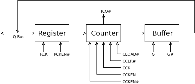
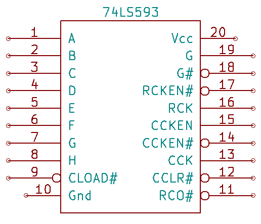
The 74LS593 is composed of three sections: a register connected to a tri-state bus (the Q bus, pins 1-8), a counter which can increment and an octal buffer which can either output the counter's value or go high-Z.
When RCKEN# is low, the register will load the value on the Q bus when RCK goes high. In other words, RCKEN# is level-triggered and RCK is edge-triggered. The register value is not visible outside the 74LS593.
The counter can do several things:
CCLR# is active low and level-triggered. When it is low, it resets the counter value to all zero bits. CCLR# has priority over CLOAD#.
CLOAD# is active low and level-triggered. When it is low, it loads the register value into the counter.
The lowest priority group of control lines are CCK, CCKEN and CCKEN#. CCK is edge-triggered. When CCK goes high, the counter is incremented. This is controlled by the level-triggered CCKEN and CCKEN#. If CCKEN is high or CCKEN# is low, then a rising CCK will increment the counter.
The 74LS593 can be cascaded to form a 16-bit, 24-bit etc. counter. When the counter's value is 11111111, the RCO# line goes low. You can wire RCO# output from the low 74LS593 up to the CCKEN# input on the next highest 74LS593 to propagate the carry. However, this is only true if the two chip share the same CCK and CCKEN, and the lower CCKEN# is high to ensure that it has no effect. See below.
The output of the counter is passed to the octal buffer which is controlled by G and G#. The only time that the counter's value is placed on the Q bus is when G is high and G# is low. For all other values of G and G#, the buffer outputs a high-Z value.
Easy. Pull CCLR# low at any time.
Choose one of CCKEN and CCKEN# to be your control line and wire CCK up to a clock signal. Example: wire CCKEN# high (so it has no effect), wire CCK to the system clock. Now when CCKEN goes high, the counter will increment on the next rising clock edge.
I beat my head against this for a while before I understood the structure of the 74LS593. Oh, and also, the datasheets are wrong. To load the counter from the Q bus, the value must firstly pass through the register. Here is what works.
Firstly, make sure that G and G# disable the counter's output if you are trying to load the counter from some other device on the Q bus.
Wire CLOAD# and RCKEN# together. This will set the register up to load from the Q bus and set the counter up to load from the register.
While they are low, raise RCK. This loads the Q bus value into the register and, because CLOAD# is low, also loads the register's value into the counter. Once RCK goes high you can raise CLOAD# and RCKEN#, but do this after some time to deal with the propagation delays with the register and counter.
I actually keep RCKEN# wired low and wire RCK to a continuous clock signal. This means that the register is always loading a value from the Q bus on the rising clock edge. Then when I need to load the counter, I drop CLOAD# beforehand and raise it afterwards.
Hint: wire CCK and RCK to the inverse of the system clock and raise/lower the CLOAD#, G, G#, CCKEN and CCKEN# lines on the rising edge of the system clock. The control lines will change at the start of the clock cycle and the counter will change in the middle of the clock cycle.
I'm using two 74LS593s in a CPU design where the pair act as a 16-bit program counter (PC). The design is microcoded so that, on the first microinstruction, the instruction register IR is loaded with the instruction and the PC is incremented. The two 74LS593s share the same CCK, and the RCO# from the lower chip is tied to CCKEN# on the higher chip.
When I reached the 16-bit PC value of 0x00FF and the PC was incremented, it incremented to 0x0200 instead of 0x0100. The reason is that the instruction had multiple microinstructions, and the lower 74LS593 stayed at 0xFF on two microinstructions. This kept RCO# low across two clock cycles, and thus the higher 74LS593 incremented on two CCK rising edges to go from 0x00 to 0x02.
My solution is to wire the counter lines as follows:
The low chip has CCK always clocked, but it can only increment when CCKEN (PCincr) goes high. The high chip can always increment, but the rising clock edge to make this happen is the rising RCO# signal from the low chip. And this only occurs when the low chip goes from 0xFF (RCO# low) to 0x00 (RCO# high). So it doesn't matter how many clock cycles the low chip stays at 0xFF, it ensures the high chip only increments on the low value resetting to 0x00.
Now that I have my CSCvon8 CPU working and I've bought a decent logic analyser, I can document how I wired up the two 74LS593s in my CPU and show the actual waveforms as they do their job.
Here is the schematic section with the two 74LS593s:
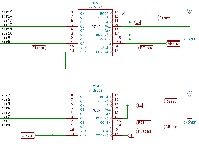
Note that many of the control lines are tied high or low. Both low and high chips are clocked by the inverse of the system clock, Clkbar#. In my design, ROMs generate the control lines and these are not guaranteed to be ready until the middle of the clock cycle. So the 74LS593 will change state mid-cycle when Clkbar# goes high.
There are three CPU control lines related to the 74LS593s:
The CPU is microcoded, so each instruction consists of several microinstructions which set or clear the various control lines. The following short program demonstrates all the above control lines:
# 21 microinstructions
#
start:  NOP                     # MEMresult IRload PCincr
                                # uSreset
        LCA '1'                 # MEMresult IRload PCincr
                                # MEMresult Aload PCincr
                                # uSreset
        JOU .                   # MEMresult IRload PCincr
                                # MEMresult AHload PCincr
                                # MEMresult ALload PCincr
                                # JumpNoTx ARena
                                # uSreset
        OUT A                   # MEMresult IRload PCincr
                                # ALUresult A
                                # ALUresult A IOload
                                # uSreset
        NOP                     # MEMresult IRload PCincr
                                # uSreset
        JMP start               # MEMresult IRload PCincr
                                # MEMresult AHload PCincr
                                # MEMresult ALload PCincr
                                # ALUresult 0 ARena JumpZero
                                # uSreset
The instructions are:
On the right are the microinstructions for each instruction; these show which control lines are enabled for each microinstruction.
Here are the waveforms sampled by the logic analyser for one loop iteration. The CPU is running at 1MHz, so each clock cycle is 1us.
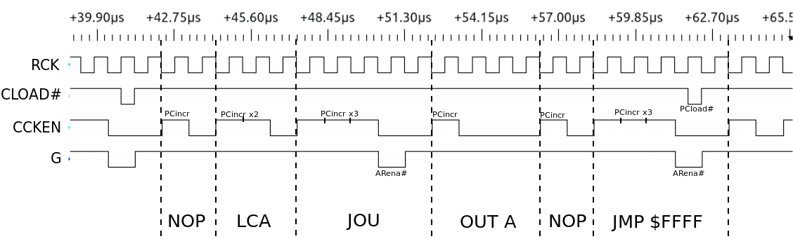
RCK (and one of the CCKs) is tied to the inverse of the system clock. I've shown each instruction starting on the falling edge of RCK as this is the rising edge of the system clock.
For all instructions, you can see CCKEN go high when the PC needs to increment. I've labelled these with PCincr, the name of the CPU control line. Each time RCK rises with CCKEN high, the PC increments. Otherwise, the PC's value stays constant.
There are two jump instructions in each loop, JOU and JMP. In the waveforms shown, JOU is not taken. The jump address is asserted on the address bus just in case. This is shown by G's low value in both jump instructions. I have labelled these with ARena#, the name of the CPU control line.
Only the JMP instruction causes the PC to load a new value. This is shown by the low CLOAD# value. Again, I have labelled this with PCload#, the name of the CPU control line.
This circuit, the short program and the waveform diagram shows how to wire up a pair of 74LS593s to: