19th April 2019
I had a realisation a couple of days ago that, in my microcoded CPU where all the control lines are generated by a instruction decode ROM, that some control lines will go to level-triggered inputs. However, some will go to edge-triggered inputs.
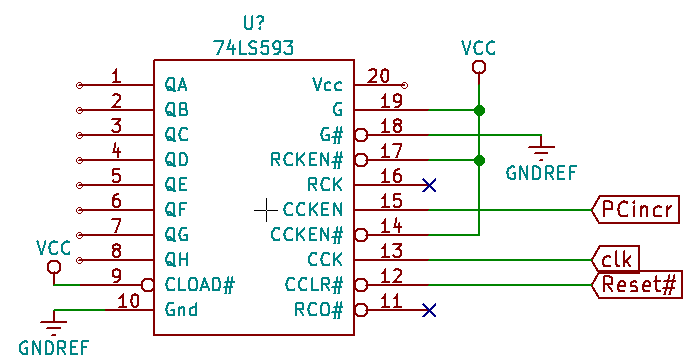
One of the latter is PCincr whose job is to increment the PC which is composed of the two 74LS593 chips. Now, in my microcode sequences, I want to increment the PC in consecutive microinstructions. An example is LCA which loads a value for A from the next byte after the instruction byte. The microsequence to do this is:
This is all fine and good except that PCincr will rise on the first microinstruction and stay high in the second one. If this is connected to an edge-triggered line, we will only see a single PC increment.
Also remember that there is a delay between the microsequencer changing the phase number (sequence 0, sequence 1) and the ROM outputting its new value. The AT27C1024 ROM that I'm using has a 45nS read time. I had thought about combining the system clock with the ROM output (e.g. with an AND gate) to form the clock signal, but the delay is going to prevent this.
Instead, here is what I'll try. I'll wire the system clock to CCK on the PClo chip, and PCincr to the CCKEN line. Here is the circuit that I've just breadboarded:
The PCincr line comes from the ROM and so is delayed when compared to the system clock. I first tried to simulate this in Icarus verilog. Here is the resulting waveform:
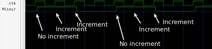
I've annotated the transitions. What is going to happen is that, if a microinstruction requests a PC increment with PCincr, it won't happen until the next clock cycle, because the clock rises before PCincr goes high.
The waveform shows an instruction like LCA with two increments, followed by two clocks with no increment, then another two increments.
The question is, is this going to cause problems? Going back to the LCA microsequence:
The Aload, like PCincr comes out of the decode ROM, so it is delayed compared to the system clock. So the PC will increment on the rising clock edge which is before Aload occurs.
But now there's another problem. Aload goes to a 74HCT574 register and it's edge-triggered. That's fine as I'm not going to load A on successive microinstructions. However, the ROM used for main memory is an AT28C256-15PU. This has a 150nS read delay. And this might cause problems as follows.
So: PCincr is high from the first microinstruction. The clock goes low and then rises. This sends CCK high and the PC increments, thus changing the address bus value. 150nS later, the new memory value arrives on the data bus.
At the same time that the clock goes high, the microsequencer changes to the next phase number. This causes the address to the decode ROM to change. 45nS later, Aload goes high and A reads the databus value. But the Aload delay is only 45nS whereas the databus delay is 150nS. So it's likely that the A register will load the wrong value from the data bus.
Sounds like I need to model this, and also do some breadboard tests. Sigh.
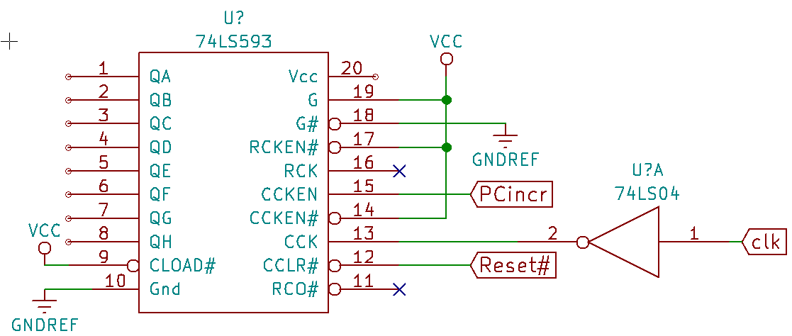
I've had an idea. If I invert the system clock, then CCK will occur when the system clock falls. Here is the circuit that I just wired up:
and here is the simulated waveforms:
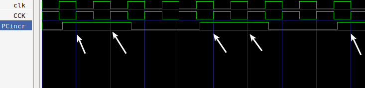
The arrows show where the PC increments will occur. This really looks promising. The PC increments well before the second rising clock when PCincr (and Aload) are high, and so the value on the data bus should have changed well before the next clock rise.
Even better, the PC changes value in the same clock cycle and not at the beginning of the next clock cycle. I think this is just making me happy and the circuit couldn't care less!
I've got my PClo 74LS593 wired up like this in my (simulated) CPU:
The simulated CPU has suitable ROM and other component delays as per the datasheets, and it does seem to be working.