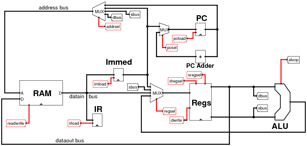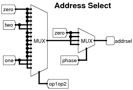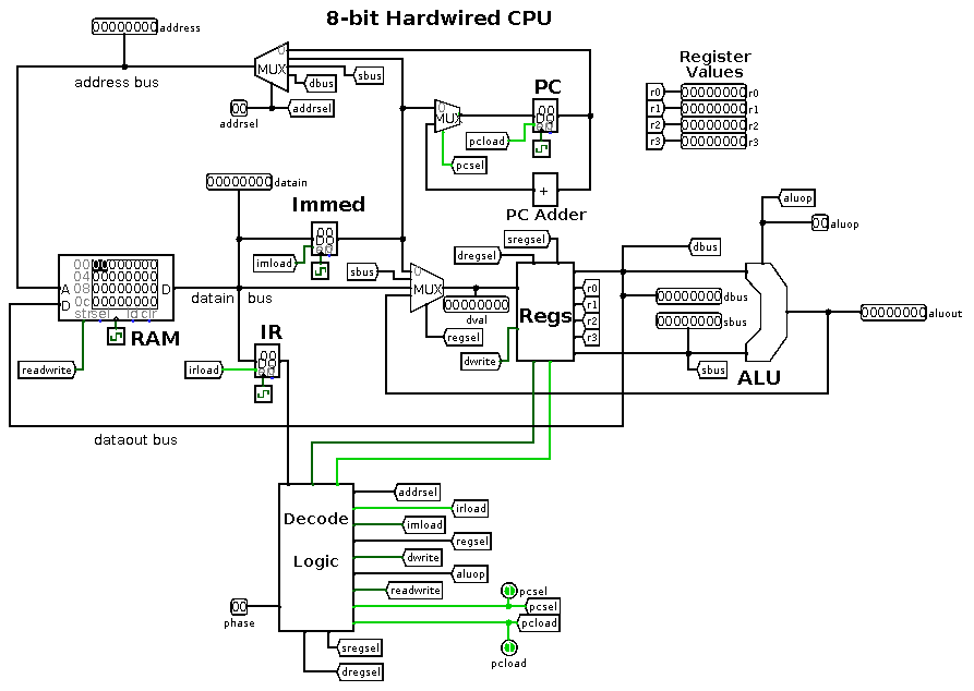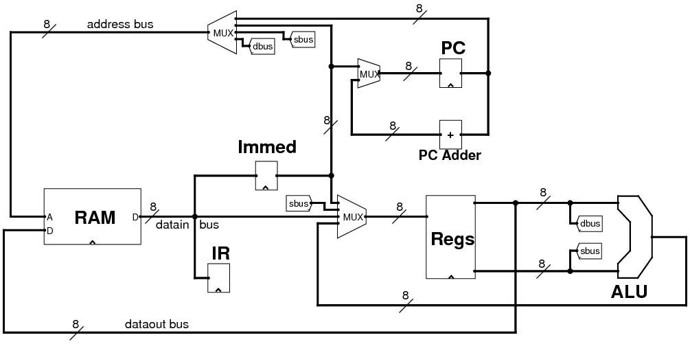
- the address bus multiplexor can get a memory address from the PC, the immediate register (for direct addressing), or from the source or destination registers (for register indirect addressing).
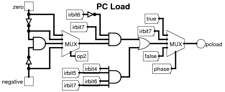
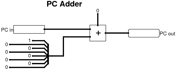
- the PC multiplexor either lets the PC increment, or jump to the value in the immediate register.
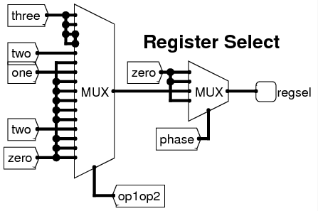
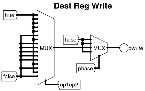
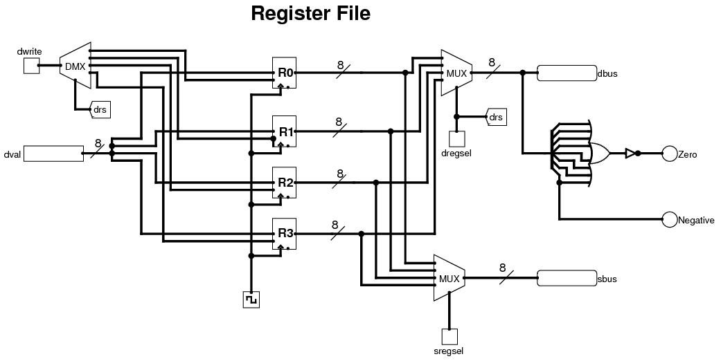
- the multiplexor in front of the registers determines where a register write comes from: the ALU, the immediate register, another register or the data bus.